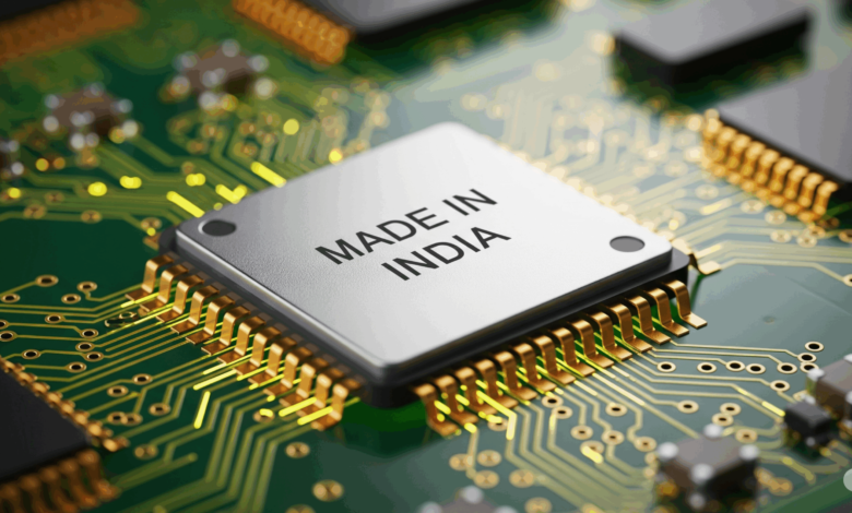
India’s semiconductor ambition is no longer a policy slogan – it is quietly becoming an economic reality. For decades, India supplied the brains to the world’s biggest chip companies, but rarely owned the intellectual property. That equation is now changing. And at the heart of this transformation lies the Government of India’s Design Linked Incentive (DLI) Scheme – a decisive intervention that is reducing risk, catalysing innovation and attracting serious capital into deep-tech semiconductor design.
Before 2021, venture capital investment in semiconductor chip design in India was limited. The reason was simple. Semiconductor ventures demand long gestation cycles, heavy R&D expenditure, sophisticated design tools and high technical risk before a single rupee of revenue flows in. For early-stage investors, that combination often appeared daunting. Hardware is not software. You cannot pivot overnight. Silicon does not forgive mistakes.
The DLI Scheme, announced in 2022, addressed this structural challenge head-on. By providing financial support, access to advanced Electronic Design Automation (EDA) tools, IP cores and centralised infrastructure such as the ChipIN Centre, the government reduced upfront risk while enhancing ecosystem credibility. Startups are not casually admitted. They undergo rigorous screening and evaluation by an expert committee comprising technical and industry specialists. This structured approach ensures that support flows to serious deep-tech companies, not speculative ventures.
The result: Investor confidence has begun to rise. Venture capital is no longer merely curious about semiconductor design in India – it is actively evaluating and backing DLI-supported startups.
A powerful example of this shift is C2i Semiconductors.
Incorporated in Bengaluru on 5 June 2024, C2i was founded by a team with decades of experience at global giants such as Texas Instruments, National Semiconductor and Maxim Integrated. This is not a startup built on aspiration alone; it is built on accumulated semiconductor wisdom. Approved under the DLI Scheme effective 1 November 2024, C2i received financial support and access to advanced chip design tools – a critical boost during its formative stage.
The presence of semiconductor industry veteran Ganapathy Subramanyam, Founding Managing Partner at Yali Capital, on its Board further strengthens its credibility. Today, C2i’s engineering team has ramped up rapidly to 65 engineers. Remarkably, the company has emerged as one of the top three users among 100 companies of the centralised EDA tools provided through the ChipIN Centre grid under the DLI Scheme. That statistic alone signals seriousness, technical depth and execution velocity.
But what problem is C2i solving?
The world’s digital infrastructure is undergoing a seismic shift. Artificial Intelligence workloads are expanding exponentially. Modern AI data centres require enormous and highly stable power supply systems. The older power architectures were never designed for continuous, high-density AI computing. The consequences are clear: energy loss, excessive heat generation, reliability challenges and difficulties in scaling infrastructure.
In today’s AI-driven world, power has become the limiting factor.
C2i Semiconductors is rethinking power delivery from the “grid to core.” Instead of merely improving isolated components, the company is building a smart, configurable power platform that intelligently manages electricity flow from the incoming power source all the way to the processor chip. This system-level innovation ensures stable power delivery even during heavy AI workloads.
In simple terms, C2i is building an intelligent power brain for AI infrastructure.
Its technology optimises power delivery in real time, improves energy efficiency, reduces heat, minimises failure rates, extends GPU and equipment lifespan, simplifies server architecture and enables faster data centre deployment. In a world where AI clusters consume megawatts of energy, such innovation is not incremental – it is transformational.
C2i expects its first silicon designs to return from fabrication by mid-year, after which performance validation will begin. This is the critical milestone every semiconductor startup must cross – proving that design brilliance translates into silicon reliability.
Investors have taken notice.
Peak XV Partners (formerly Sequoia Capital India & SEA) has led a $15 million investment round in C2i to accelerate the development of next-generation, high-density and ultra-reliable power delivery solutions. This follows a $4 million round led by Yali Capital in 2024. Together, the cumulative investment now stands at approximately ₹170 crore, in addition to the support provided under the DLI Scheme.
Rajan Anandan, Managing Director at Peak XV, has highlighted that C2i’s approach to power management can significantly extend GPU lifespan and unlock billions of dollars in industry savings. That statement reflects more than optimism – it reflects commercial logic. In AI data centres, marginal efficiency improvements translate into massive economic gains.
This convergence of policy support and private capital is not accidental. It aligns directly with the broader semiconductor vision articulated by Union Minister Shri Ashwini Vaishnaw. India’s semiconductor programme is not limited to manufacturing fabs; it is equally committed to strengthening design capabilities, building domestic intellectual property and nurturing globally competitive product companies.
India already possesses one of the strongest chip design talent bases in the world. Thousands of Indian engineers design chips for multinational corporations. The government’s role is now to ensure that this talent also builds Indian IP, Indian companies and Indian semiconductor champions. Through design incentives, access to advanced tools, IP frameworks and ecosystem support, startups can scale into global technology leaders.
C2i represents precisely that model – a design-led deep-tech company born in India, backed by global investors and supported by a strategic national policy.
For too long, India was seen as the back office of global semiconductor design. The DLI Scheme is enabling India to become the front office – owning patents, products and platforms. Deep-tech innovation requires patience, capital and conviction. With DLI reducing early-stage risk and investors stepping in with growth capital, the semiconductor design ecosystem is entering a virtuous cycle.
If this trajectory continues, India will not merely participate in the global semiconductor supply chain – it will shape it.
The story of C2i Semiconductors is therefore not just about power management chips for AI data centres. It is about policy meeting entrepreneurship. It is about reducing systemic risk to unlock private capital. It is about transforming India from a talent supplier to a technology owner.
Semiconductor sovereignty is not built overnight. But it is built through companies like C2i – one design, one silicon tape-out, one innovation at a time.